Via Stitching in RF PCB Design: Essential Guide for Signal Integrity
N/A, Thursday, 28 November 2024.
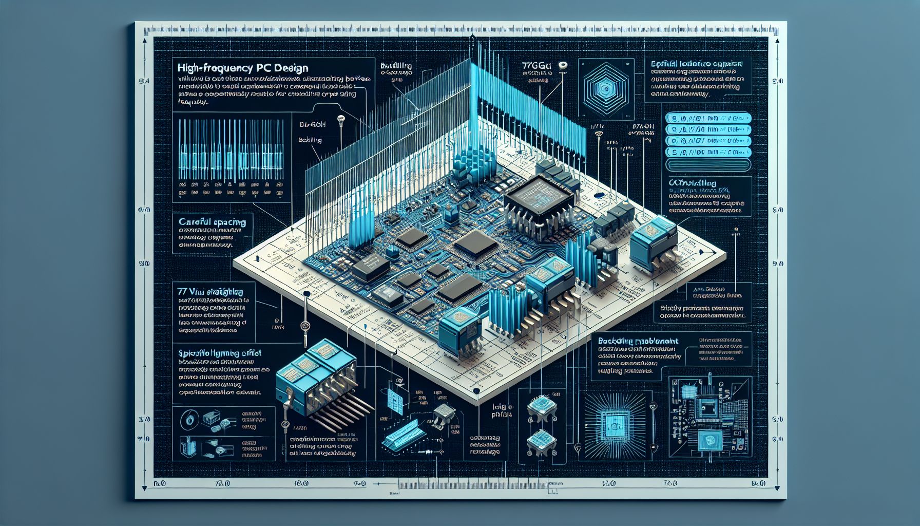
High-frequency PCB designs require careful via stitching implementation, with optimal spacing between vias at λ/20 to λ/10 of the operating frequency. Proper stitching is crucial above 3-5 GHz, where conventional design calculators fail. For 77 GHz radar modules, specialized techniques including backdrilling and strategic placement become essential for maintaining signal integrity.
Understanding the Role of Via Stitching
In the intricate world of RF PCB design, via stitching emerges as a pivotal technique to manage signal integrity and electromagnetic interference (EMI). As frequencies rise above 3 to 5 GHz, the impedance of vias starts to deviate significantly, demanding a meticulous approach to maintain a coherent signal path. Via stitching involves placing multiple vias strategically across the PCB, connecting different copper layers to ensure a robust ground return path and mitigate signal distortion.
Practical Applications in High-Frequency Designs
For high-frequency applications such as 77 GHz radar modules, the stakes are particularly high. These systems often require a grounded coplanar waveguide with precise via spacing to suppress unwanted frequencies and enhance isolation. By implementing backdrilling techniques, designers can further minimize signal reflections and maintain the desired impedance. This is crucial in preventing parasitic effects that can degrade performance in high-frequency environments[1].
Applying Via Stitching in DIY Electronics
For DIY enthusiasts venturing into RF PCB projects, understanding via stitching can significantly enhance project outcomes. Whether using constant ground via or shielding via stitching techniques, the goal is to maintain low resistance and efficient heat dissipation. Ground planes are often stitched to prevent ground bounce issues, a common pitfall in DIY projects that can lead to circuit failures. By applying these techniques, hobbyists can achieve professional-level performance in their PCBs[2].
Resources for Further Learning
Aspiring RF PCB designers can delve deeper into the world of via stitching through various online resources. Websites like PCB Hero offer detailed guides on RF PCB layout and routing, while forums such as Reddit’s r/PrintedCircuitBoard provide community-based insights and troubleshooting tips. Additionally, webinars and online courses focusing on high-frequency PCB design can equip learners with the necessary skills to excel in this challenging field[3].