Circuit Board Revolution: Ultra HDI Technology Takes Center Stage
Worldwide, Thursday, 24 October 2024.
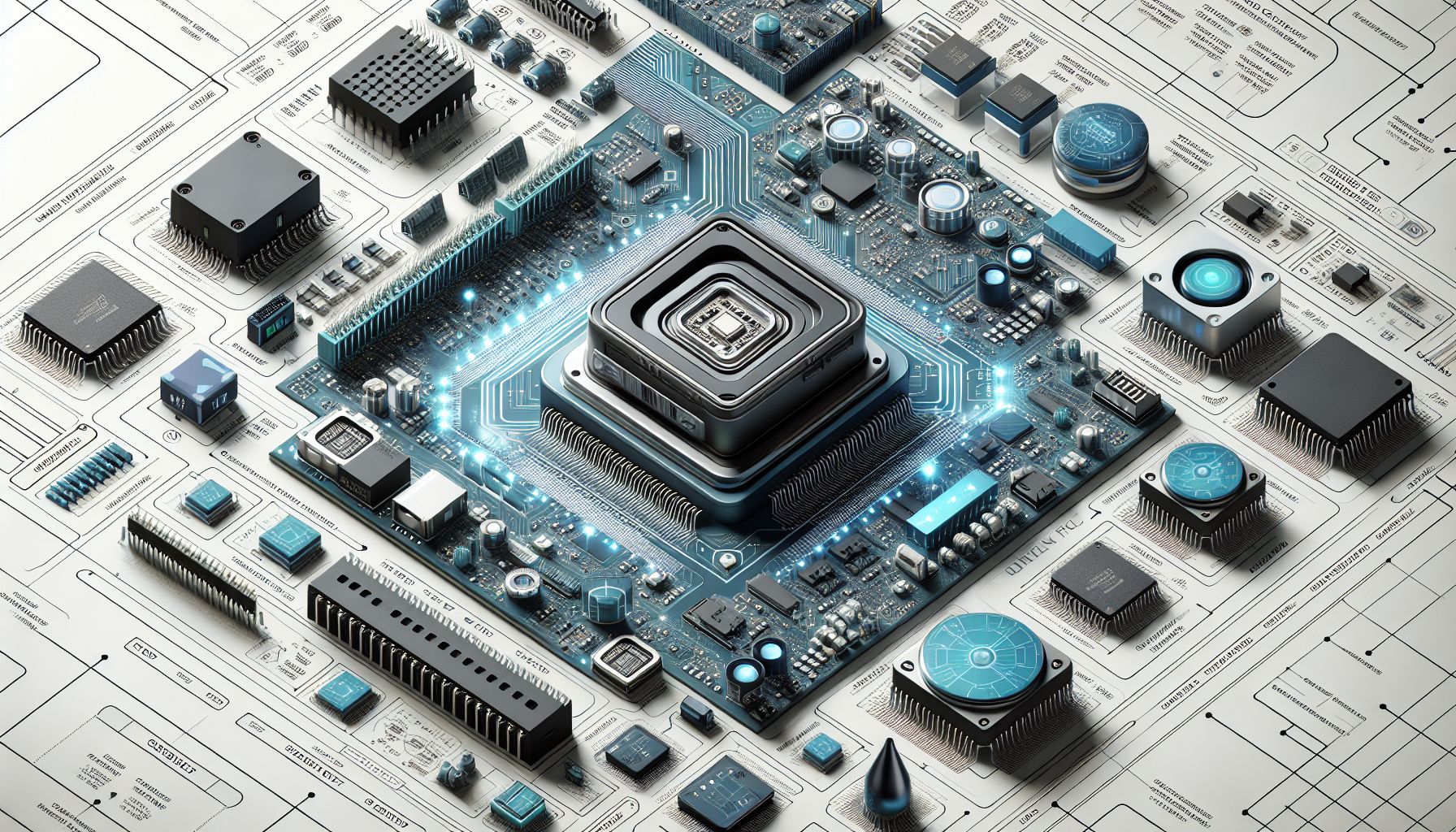
The electronics industry is witnessing a paradigm shift as Ultra High Density Interconnect (UHDI) technology emerges as a game-changer in circuit board design. This advanced approach promises unprecedented miniaturization and performance improvements, addressing the growing demands of complex electronic systems in an increasingly compact world.
Emergence of UHDI Technology
As the demand for more compact and efficient electronic devices escalates, Ultra High Density Interconnect (UHDI) technology is making waves in the circuit board industry. UHDI enables designers to pack more functionality into smaller spaces, essential for next-generation applications such as 5G, IoT, and advanced computing systems. This leap in technology is primarily driven by the need to accommodate high Input/Output (I/O) semiconductor packaging with narrower terminal pitches, as highlighted by Vern Solberg[1].
Technological Innovations at SMTA International
The recent SMTA International 2024 event showcased the groundbreaking advancements in UHDI technology. The introduction of the UHDI Learning Pavilion provided an interactive platform for industry professionals to delve into the intricacies of UHDI design and manufacturing. Key sessions covered UHDI Test Board Design, fabrication processes, and the use of ultra-fine solder powders, offering attendees a comprehensive understanding of the technology’s capabilities and challenges[2].
Industry Collaboration and Knowledge Sharing
A significant aspect of the SMTA event was the ‘Lab to Fab’ working session, aimed at fostering collaboration across the supply chain to accelerate the transition from concept to production. Experts like Elliott Fowler from Sandia National Laboratories emphasized the importance of breaking down silos to achieve seamless integration of UHDI technology into mainstream manufacturing processes[2].
Strategic Investments in UHDI Infrastructure
In a strategic move to bolster UHDI production capabilities within the United States, TTM Technologies has announced the construction of a new facility in Dewitt, New York. This $130 million investment, supported by a $30 million grant from the Department of Defense, aims to fill a critical technology gap in high-density printed circuit board production. The facility will enhance supply chain resilience and create 400 jobs, underscoring the importance of UHDI in national defense and technological advancement[3].
Challenges and Considerations in UHDI Implementation
Despite the promising advancements, implementing UHDI technology comes with its own set of challenges. The reliability of laser-drilled microvia-in-pad structures, for instance, has been a subject of scrutiny. Studies indicate variations in lifetime across different package types, highlighting the need for careful design and manufacturing considerations. As noted by the IPC’s High-Density Packaging User Group, factors such as aspect ratio and stacked vias significantly impact failure rates, necessitating thorough design for manufacturability (DFM) strategies[4].
Conclusion: The Future of UHDI in Electronics
The evolution of UHDI technology represents a significant stride towards meeting the ever-increasing demands of modern electronic devices. As the industry continues to innovate, the integration of UHDI into mainstream production will likely redefine the capabilities and applications of electronic systems. With ongoing investments and collaborative efforts, UHDI stands poised to transform the landscape of circuit board design, paving the way for more compact and efficient technology solutions.