Silicon Carbide Breakthrough: 300mm Wafer Unveiled at Electronica 2024
Munich, Friday, 15 November 2024.
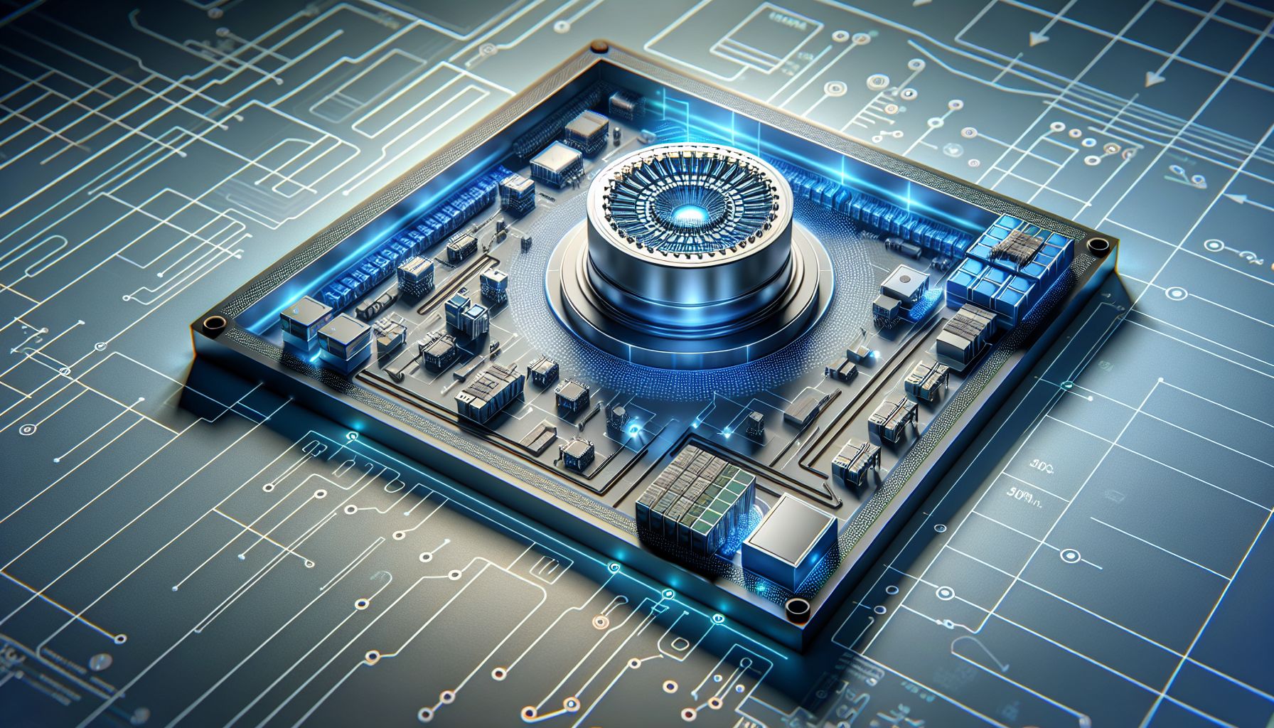
Chinese firm SICC showcases world’s first 300mm N-type SiC substrate at Electronica 2024, marking a significant leap in semiconductor technology. This innovation promises enhanced yields and performance for power electronics applications.
A New Benchmark in Semiconductor Innovation
The unveiling of the 300mm N-type Silicon Carbide (SiC) substrate by SICC at Electronica 2024 represents a pivotal advancement in semiconductor technology. The introduction of this novel substrate size is poised to transform the power electronics landscape by significantly enhancing device performance and production efficiency. With SICC’s emphasis on reducing threading screw dislocation (TSD) and basal plane dislocation (BPD) densities, this innovation is expected to yield higher reliability and efficiency in semiconductor devices, setting a new standard for the industry[1].
Implications for Power Electronics
Silicon Carbide technology is renowned for its ability to handle higher voltages and temperatures, making it ideal for applications in electric vehicles, renewable energy, and industrial power systems. The larger 300mm wafers introduced by SICC enhance these capabilities further by allowing for more powerful and efficient chips. This development aligns with the global shift towards wide bandgap semiconductors, which are anticipated to capture a significant share of the power semiconductor market by 2027[2].
Industry Reactions and Future Prospects
Industry experts see SICC’s breakthrough as a step towards meeting the growing demand for high-performance semiconductors. As companies like Navitas Semiconductor and Infineon Technologies also showcase advancements in SiC technologies at Electronica 2024, the event highlights a broader industry trend towards innovation in power electronics. The potential environmental benefits, such as reduced CO2 emissions through more efficient power conversion, further underscore the significance of these advancements[3].
Conclusion: Setting the Stage for Future Growth
The introduction of the 300mm SiC wafer not only demonstrates SICC’s technological prowess but also sets a precedent for future developments in the semiconductor industry. As demand for energy-efficient and high-performance electronic devices continues to rise, innovations like these will be crucial in driving the next wave of growth in power electronics, positioning SiC technology at the forefront of this evolution[4].