PCB Design Revolution: Skip the Schematics, Start Building Faster
Online, Saturday, 30 November 2024.
A groundbreaking shift in PCB design methodology emerges, allowing experienced engineers to bypass traditional schematic creation. This direct-to-board approach promises to slash development time while maintaining design integrity, though it requires solid expertise in circuit design. The technique, gaining traction among seasoned developers, challenges conventional PCB design workflows.
The Rise of Direct-to-Board Methodology
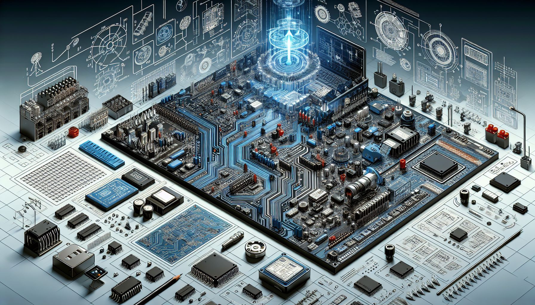
In recent years, the electronics industry has witnessed a paradigm shift in how printed circuit boards (PCBs) are designed. Traditionally, engineers relied on detailed schematics and footprints to guide their designs. However, the emergence of direct-to-board design tools has enabled experienced engineers to skip these steps, focusing instead on the layout and functionality directly. This method not only accelerates the design process but also reduces potential errors associated with translating schematic designs into board layouts. By leveraging these tools, engineers can more rapidly prototype and iterate on their designs, making it an attractive option for those with a deep understanding of circuitry.
Tools and Techniques Leading the Charge
Several software tools have been pivotal in supporting this innovative approach. KiCad, for instance, has been praised for its flexibility in allowing designers to work directly with PCB layouts without first creating schematics[1]. Other platforms like Altium and DipTrace have also integrated features that support this methodology, offering users advanced tools for direct design[2][3]. These platforms provide functionalities that enable designers to manipulate components and connections dynamically, ensuring that the integrity of the design is upheld while bypassing traditional steps.
Challenges and Considerations
While the direct-to-board approach offers numerous advantages, it is not without its challenges. This method demands a high level of expertise in circuit design, as it eliminates the safety net provided by traditional schematics. Errors in design logic or component placement can be costly, requiring a meticulous approach to ensure that designs are both functional and manufacturable. Therefore, this methodology is best suited for seasoned engineers who have a robust understanding of electronic circuits and can visualize the end product without needing intermediary steps.
Real-World Applications and Learning Resources
The practical applications of this methodology are vast, particularly in industries where rapid prototyping is crucial, such as consumer electronics and IoT devices. As more companies adopt this approach, resources for learning and mastering these techniques have expanded. Platforms like PCBWay offer tutorials and project showcases that highlight how to implement these methods effectively[4]. For engineers looking to enhance their skills, engaging with online communities and forums, such as those on Reddit, can provide insights and peer support from others who have successfully transitioned to this new design paradigm[5].
Conclusion: Embracing the Future of PCB Design
As the electronics industry continues to innovate, the direct-to-board approach represents a significant evolution in PCB design. By eliminating the need for schematics and footprints, this method empowers experienced engineers to work more efficiently and creatively. As more tools become available and the community of users grows, this approach is poised to become a staple in the toolkit of modern electronics designers, driving faster development cycles and more agile product iterations.