Decoding PCBs: A Guide for Electronics Enthusiasts
Global, Monday, 21 October 2024.
Explore the intricate world of printed circuit boards with our comprehensive guide. Learn to interpret color codes, decipher symbols, and trace circuits to enhance your electronics skills. Discover how understanding PCB layers and components can revolutionize your approach to circuit design and diagnostics.
Understanding PCB Structure
Printed circuit boards (PCBs) are the backbone of modern electronics, consisting of multiple layers that include conductive copper and insulating substrate materials. The most common substrate used is FR-4, a flame retardant composite that offers excellent electrical insulation and mechanical strength[1]. These layers enable complex circuit designs, essential for the functionality of devices ranging from simple gadgets to advanced computing systems.
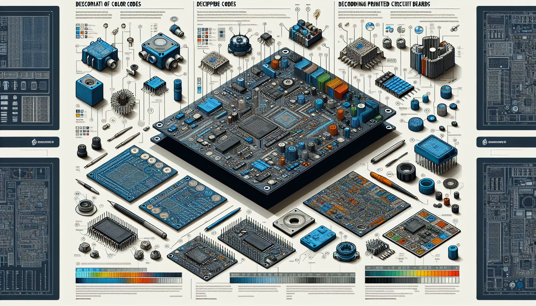
Decoding Symbols and Markings
PCBs are adorned with various symbols and markings that are crucial for assembly and diagnostics. Resistors, for instance, use color bands to denote resistance values and tolerances, such as the brown, black, orange, and gold bands indicating a 10,000-ohm resistor with a 5% tolerance[1]. Capacitors, on the other hand, might be marked with numeric codes like ‘104’, representing a capacitance of 100,000 pF or 0.1 μF. These symbols and markings are essential for ensuring correct component placement and functionality.
Tracing and Testing Connections
Tracing circuits involves following copper pathways, or traces, which connect various components on the PCB. These traces are categorized into signal, power, and ground traces, each serving specific roles in the circuit’s operation. For effective tracing, it’s important to utilize tools like multimeters and continuity testers to verify electrical pathways and identify issues such as shorts or open circuits[1]. Visual inspection techniques, including the use of magnifying tools and appropriate lighting, can also aid in detecting anomalies like burnt components or cracked solder joints.
Advanced Techniques and Tools
Advanced PCB analysis often requires the use of specialized software and testing equipment. PCB design software, such as Eagle or KiCad, allows users to visualize and analyze layouts, making it easier to trace connections and verify designs[1]. For more detailed testing, equipment like oscilloscopes and logic analyzers can provide insights into signal integrity and circuit performance. Additionally, flying probe testers and boundary scan tests are employed in mass production to ensure the quality and reliability of complex PCBs[2].
Applying Knowledge to Real-World Projects
Understanding PCBs can significantly enhance problem-solving abilities in electronics projects. By mastering the interpretation of circuit board elements, enthusiasts can design more efficient circuits, troubleshoot issues effectively, and innovate new solutions. For those seeking further learning, resources such as online tutorials, community forums, and detailed guides on platforms like Wevolver provide valuable insights[1]. Continuous practice and exploration in this evolving field will lead to greater proficiency and creativity in electronics design.