NHanced Semiconductors and University of Florida Unveil Roadmap for Chiplet Integration
Florida, Wednesday, 20 August 2025.
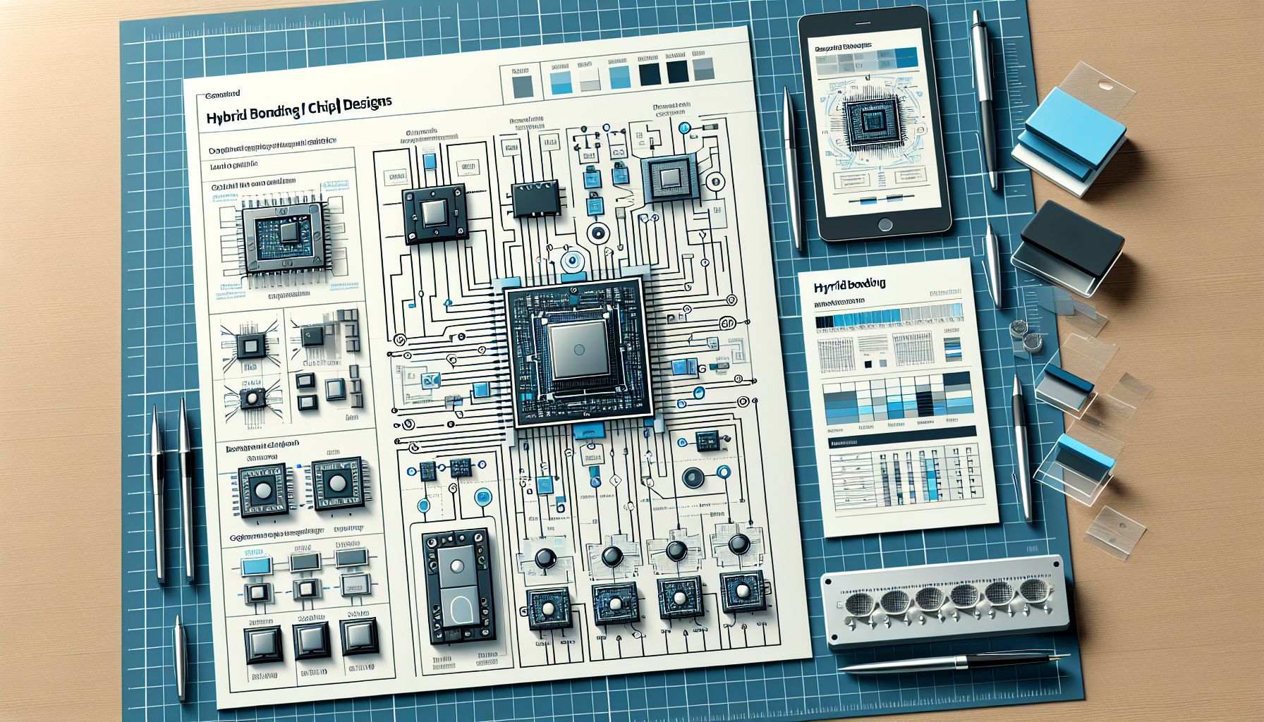
A newly presented paper offers a roadmap for using hybrid bonding in chiplet designs, which is crucial for the future of electronics manufacturing.
The Breakthrough in Chiplet Designs
At the 36th Electronics Packaging Symposium held in September 2025, NHanced Semiconductors in collaboration with the University of Florida presented groundbreaking research on the integration of chiplet architectures using hybrid bonding technology. The team offered a strategic roadmap promising enhanced electrical, mechanical, and thermal continuity for high-performance computing applications. This technology is expected to transform electronics manufacturing by deploying compact chiplets that improve processing efficiency and reduce production costs [1].
Technical Paper Highlights
NHanced’s paper highlights critical advances in hybrid bonding, addressing the semiconductor industry’s need for robust integration solutions. The document discusses the emerging ecosystem, detailing how hybrid bonding facilitates fine-pitch chiplet integration, essential for next-gen di-to-die connectivity. These innovations could significantly impact various sectors by allowing more complex chip designs without escalating costs or complexity [1].
Collaborative Efforts and Industry Impacts
The symposium, orchestrated by the Integrated Electronics Engineering Center along with industry giants like GE Aerospace and IBM Research, aims to foster innovation through collaboration. Keynote speakers emphasized the importance of combining academic research with industry expertise to address the fabrication and integration challenges posed by modern chiplet architectures. The integration of chiplets using hybrid bonding is seen as a pivotal step toward achieving high-density, scalable chip designs [1][2].
Future Implementation
While NHanced and the University of Florida’s findings are at the forefront of semiconductor innovation, practical implementation requires addressing various manufacturing challenges. Industry professionals are keen to leverage these findings to enhance chip design efficiency. As electronics continue to evolve, these advancements promise to support future developments in areas ranging from consumer electronics to military applications. Moreover, the hybrid bonding approach paves the way for enhanced microelectronics designs aligning with the global trend toward miniaturization and increased functionality [1].