PCB Design Techniques Enhance Electronic Systems' Efficiency
Global, Sunday, 8 December 2024.
Explore how effective PCB design can boost the efficiency and functionality of electronic systems, offering valuable insights for both engineers and DIY enthusiasts.
Modern PCB Design Fundamentals
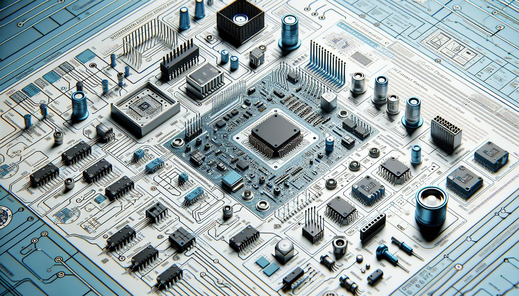
In today’s electronics landscape, PCB design has evolved to meet increasingly complex demands. High-frequency circuit boards now commonly operate at frequencies ranging from hundreds of MHz to several GHz [4], requiring sophisticated design approaches for optimal performance. Modern PCBs are essential components in various industries, from telecommunications to medical devices, with a particular focus on signal integrity and thermal management [3]. The efficiency of electronic systems heavily depends on PCB and PCBA technologies, which are crucial for electrical connections and overall system performance [2].
Key Design Considerations for Optimal Performance
Effective PCB design requires careful attention to several critical factors. Thermal management is paramount, with strategies including copper trace design for heat conduction and the integration of thermal vias for effective heat transfer [2]. For high-frequency applications, controlled impedance routing (typically 50 Ω or 75 Ω) is essential for maintaining signal integrity [4]. Material selection plays a crucial role, with high-quality substrates like FR-4 and aluminum-core PCBs being preferred for different applications based on their specific requirements [2][3].
Advanced Techniques for Signal Integrity
Signal integrity in modern PCB design demands sophisticated approaches. Key techniques include differential pair routing to reduce electromagnetic interference and maintaining consistent trace widths for optimal performance [3]. For high-frequency applications, designers must focus on minimizing parasitic effects and choosing appropriate layer stack-ups [3]. Recent developments as of late 2024 show an increasing emphasis on controlled impedance and advanced shielding techniques to mitigate EMI for clearer signal transmission [4].
Future Trends and Best Practices
The field of PCB design continues to evolve rapidly. Recent trends as of December 2024 indicate a growing focus on automation and new materials [3]. For beginners entering the field, starting with simpler projects like NFC-enabled designs before progressing to more complex ones is recommended [1]. Industry experts emphasize the importance of thorough testing and validation procedures, including network analysis and electromagnetic field simulations, to ensure designs meet current standards [3].