Troubleshooting PCB Design: A Guide for DIY Electronics Enthusiasts
Mountain View, Friday, 15 November 2024.
Explore common issues in PCB design for DIY electronics projects. Learn diagnostic approaches and solutions for both hobbyists and professionals. Discover how to identify and resolve malfunctions in complex circuit designs.
Understanding PCB Design Challenges
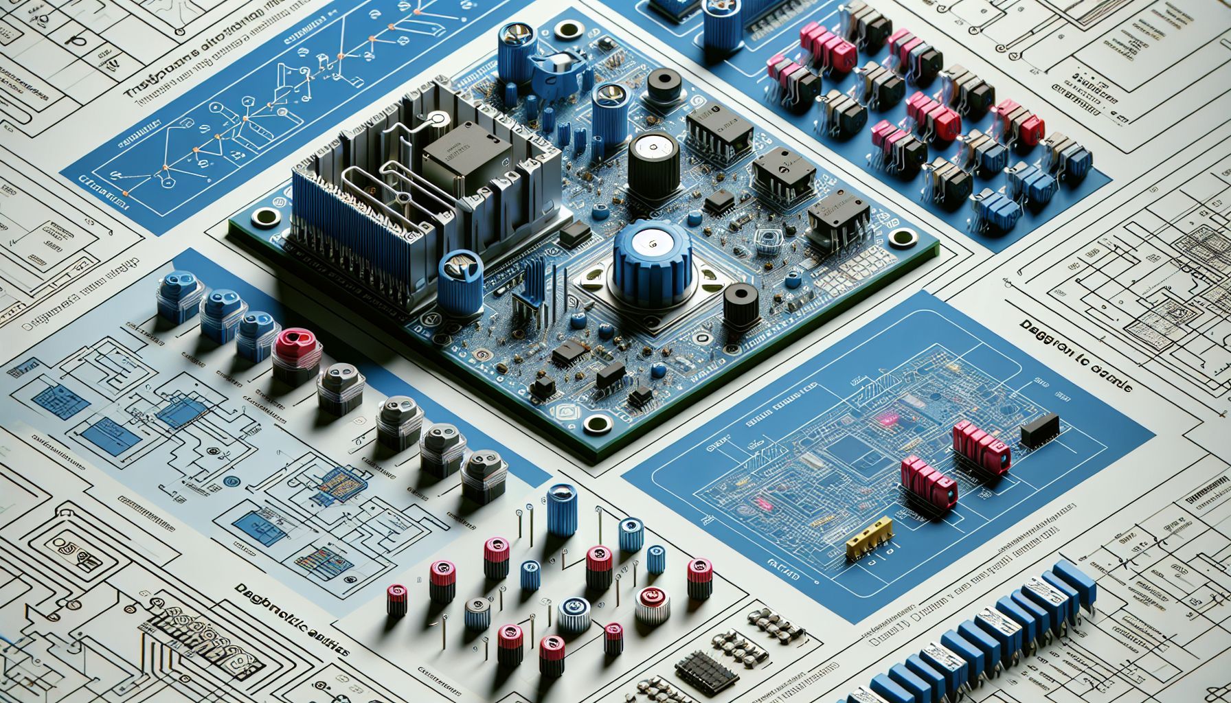
Printed Circuit Board (PCB) design can be a formidable task, particularly for DIY electronics enthusiasts venturing beyond breadboards into more sophisticated, compact assemblies. The allure of creating a custom PCB lies in its promise of greater reliability and efficiency, yet this path is strewn with potential pitfalls. Issues often arise from component placement, trace routing, and power distribution, leading to malfunctions that can baffle even seasoned hobbyists.
Common Issues and Diagnostic Strategies
One prevalent issue in PCB design is improper power distribution, which can result in components not receiving adequate power, leading to erratic behavior or complete failure of the board. This is often exacerbated by poor soldering connections or thermal management, particularly when high-power components are involved. For instance, in a recent forum discussion, a hobbyist reported issues with motor drivers burning out when switching from an 18V to a 24V power supply, highlighting the importance of considering voltage ratings and thermal dissipation[1].
Step-by-Step Diagnostic Approach
To effectively diagnose PCB issues, a structured approach is crucial. Begin by visually inspecting the board for obvious defects such as broken traces or poor solder joints. Use a multimeter to check for continuity and proper voltage levels across the board. Comparing the actual performance of components, such as current and voltage measurements, against their specifications can reveal discrepancies. In the case of malfunctioning motor drivers, one might isolate these components to test if their removal stabilizes the circuit, as was found in a real-world example where removing specific drivers improved circuit stability[1].
Solutions and Best Practices
Once the problematic area is identified, solutions can be tailored accordingly. For power distribution issues, ensuring that power traces are sufficiently wide and that decoupling capacitors are used near power pins can mitigate voltage drops and noise. Thermal management can be improved by adding heat sinks or using thicker copper layers. Additionally, adopting a robust design workflow that includes simulation tools and a thorough prototyping phase can preempt many issues. A contributor on a PCB design forum recommended isolating high-current paths to prevent electromagnetic interference with sensitive components[2].
Conclusion: Navigating the PCB Design Landscape
Navigating the intricacies of PCB design requires patience, precision, and a willingness to learn from each iteration. By adopting a methodical approach to troubleshooting and incorporating best practices from experienced professionals, DIY enthusiasts can overcome common hurdles and achieve reliable, efficient circuit designs. This not only enhances the performance of their projects but also deepens their understanding of electronics design.