Mastering the Leap: Navigating 6-Layer PCB Design Challenges
Online, Sunday, 17 November 2024.
Transitioning from 4 to 6-layer PCBs offers enhanced performance but presents unique design hurdles. Key considerations include optimal layer stack-up, ground plane separation, and via management. This shift demands a strategic approach to maintain signal integrity and minimize electromagnetic interference in complex electronic designs.
Understanding the Benefits of a 6-Layer PCB
Upgrading from a 4-layer to a 6-layer PCB can significantly improve the performance of electronic circuits, primarily by enhancing signal integrity and reducing electromagnetic interference (EMI)[1]. The additional layers allow for more intricate routing, which is essential for complex designs where high-speed signals are present. By incorporating an extra ground plane and signal layer, designers can achieve better isolation between analog and digital circuits, mitigating noise issues and improving overall functionality[1].
Layer Stack-Up Considerations
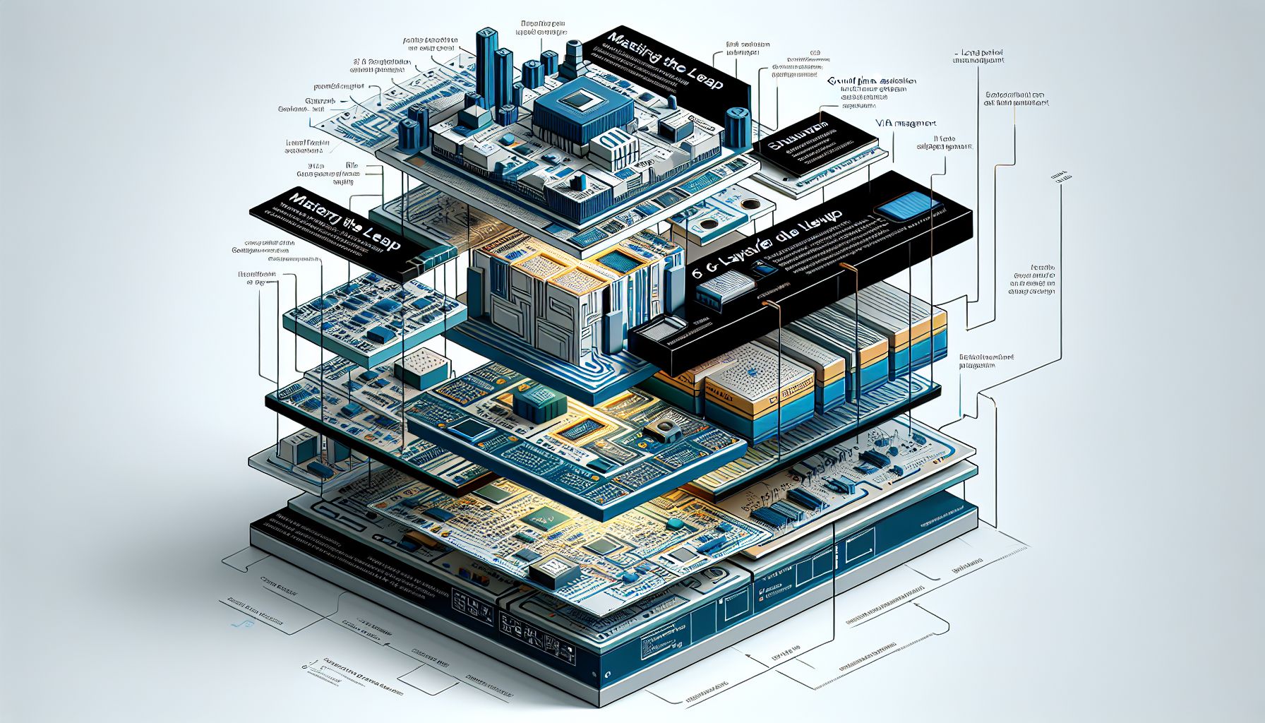
The configuration of a 6-layer PCB generally includes two signal layers, a ground plane, a power plane, and additional layers for routing[1]. An optimal stack-up might arrange these as: top signal, ground plane, inner signal, power plane, another inner signal, and bottom signal. This setup enhances return paths for signals and helps manage EMI, crucial for maintaining signal integrity in high-performance applications[1]. Proper layer stack-up is vital as it affects cross-talk, impedance control, and thermal management.
Separating Analog and Digital Grounds
One of the critical challenges in transitioning to a 6-layer PCB is effectively separating analog and digital grounds[2]. This separation minimizes interference between sensitive analog signals and noisy digital circuits. Typically, these grounds should meet at a single point near the power supply entry to prevent ground loops[1]. Utilizing separate ground planes for analog and digital circuits can further enhance performance by providing dedicated paths for return currents and reducing potential noise interference.
Via Management and Copper Pour Techniques
Incorporating additional layers requires careful via management to connect different layers without compromising the integrity of the ground planes. Blind and buried vias can be used to maintain signal paths without exposing them to external layers, although not all manufacturers support these options[3]. Copper pour on signal layers should connect to the respective ground plane using via stitching, ensuring that it does not reduce copper coverage significantly[2]. Strategic via placement is essential to maintain the efficiency of the 6-layer design.
Best Practices for 6-Layer PCB Design
To maximize the benefits of a 6-layer PCB, several best practices should be followed. Firstly, maintain clear separation between the ground planes and ensure they only connect at a single strategic point to avoid interference[1]. Secondly, use controlled impedance traces to manage signal integrity, especially in high-frequency applications. Lastly, rigorous testing and validation are essential to confirm the performance and reliability of the PCB design, particularly in reducing EMI and maintaining signal clarity[1].